2 min.
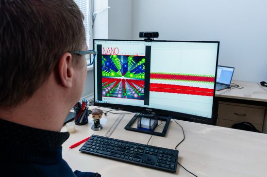

The scientists from the Department of Physics at the Faculty of Science, University of Ostrava (PřF OU) – Nilesh Kumar, Miroslav Kolos, and František Karlický – previously focused their research on a pair of two-dimensional materials: boron phosphide and chromium diselenide. Each material has unique optical and electronic properties, but it was the combination of these materials into a so-called van der Waals heterostructure that revealed the true potential of the system.
“We discovered that even a tiny shift in the relative positioning of the material layers – by just the distance of a single atom – can drastically change its optical properties. We don’t need any impurities, chemical modifications, or mechanical deformations. It’s like playing with building blocks, where shifting a single piece results in an entirely different function,” explains Dr. Miroslav Kolos from the Department of Physics, Faculty of Science, University of Ostrava.
Metaphorically speaking, the scientists found a way to control what a material absorbs – simply by altering its geometry. Certain layer configurations allow the absorption of light across a very broad spectrum, opening the door to new types of photodetectors, energy-efficient solar cells, and quantum communication components.

Light absorption is associated with the creation of so-called excitons, which refer to a pair consisting of a detached electron and the hole left behind. In some cases, the electron is in one material layer, while the hole is in the other – a phenomenon referred to as interlayer excitons.
“It’s fascinating to observe how two layers, even though they are not chemically bonded, create a new quality in the heterostructure, almost like a switch. The material we designed is exceptional in terms of the equal distance between atoms in both layers. This allows the layers to fit together precisely, and the weak interaction between them ‘switches’ to another mode. It turned out that in some configurations, interlayer excitons occur, while in others, they do not. This results in different absorption of solar radiation,” adds Associate Professor František Karlický, head of the team at the Department of Physics, PřF OU.
The discovery by the physicists from Ostrava, described in the prestigious Nano Letters journal, offers future possibilities for effectively controlling how a material interacts with light or other electromagnetic radiation – all through the precise arrangement of its layers at the atomic level. This approach could eventually lead to the development of entirely new components with predefined properties, extending far beyond the current boundaries of electronics. In practice, such a material could enable the creation of cheaper, more energy-efficient, and higher-performance devices in the fields of solar energy, optics, and quantum communication. The significance of the discovery is further highlighted by the fact that it was featured on the cover of the journal issue.
This is another outcome of the strategic project Life Environment Research Center Ostrava (LERCO), reg. no. CZ.10.03.01/00/22_003/0000003, which is one of the tools enabling the transformation of the Moravian-Silesian Region from a “coal-based” to a “healthier and smarter” region.